home / news / Industry Applications

Industry Applications | How should the thickness of semiconductor wafers be measured?

2023-08-17
    Share to


In recent years, with the continuous development of 5G technology, Internet of Things, and science and technology, the demand for semiconductor wafer industry is increasing. General wafer thickness has certain specifications, and wafer thickness has an important impact on the performance and quality of semiconductor devices. The continuous development of integrated circuit manufacturing technology, chip feature size is also gradually reduced, leading to the rise and development of wafer thinning process, wafer thickness measurement has become one of the necessary needs of many wafer manufacturers.

Wafer Preparation Flow


Currently, the main preparation processes for wafers are: single crystal growth, slicing, polishing, deposition, making circuits, cleaning, and testing.

      Among them, testing is the key link to evaluate the quality of wafers, which helps to ensure the performance and reliability of wafers. The testing items for wafers include package testing, contact resistance testing, RF testing, defect testing, thickness testing, roughness testing, flatness testing, etc.


Development Process of Wafer Thickness Inspection


Early (1970s) wafer thickness inspection is through the contact method detection, such as: micrometers, profilometer, etc., this type of method is relatively simple and intuitive, but the measurement accuracy is low, and it is easy to cause damage to the wafer, material loss.

And then with the development and progress of science and technology, non-contact measurement has become the mainstream method of wafer thickness inspection. Among them, there are mainly white light interferometer, ray fluorescence method, laser displacement sensor, spectral confocal displacement sensor and so on. These methods measure from the microscopic level, non-contact detection through the principle of optics, will not cause damage to the wafer, and the measurement accuracy is high.

At present, the wafer thickness inspection technology has been developed to a high level, and a variety of non-contact measurement technologies continue to emerge to provide reliable technical support for the semiconductor industry. However, with the gradual shrinkage of the process node, the thickness of the wafer is also gradually becoming smaller, and the requirements for wafer thickness detection are also getting higher and higher.


Examples of Wafer Thickness Inspection


An electronics research institute wanted to detect wafer TTV thickness with an accuracy of 1μm, so as to realize automatic measurement on the production line and screen for defective products. UCOMETRIC received the customer's measurement requirements, selected and tested for the customer and customized the solution:

Atometrics engineers first tested six randomly selected points on the wafer to derive the thickness of each point on the wafer.。

The thickness variation of the wafer is then tested by moving the carrier table to simulate automatic real-time measurements.

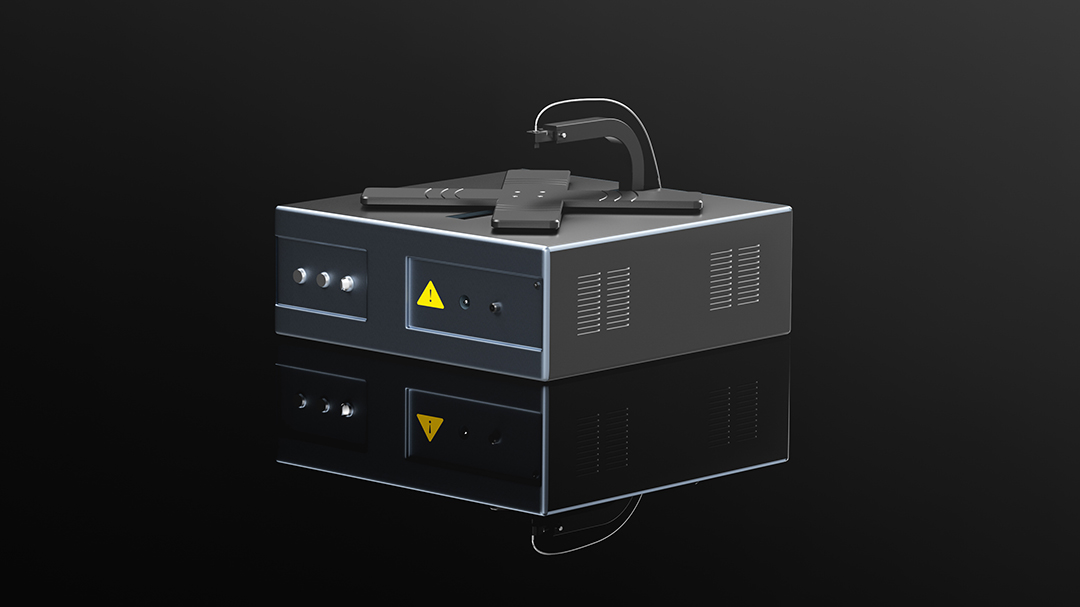
In order to meet the requirements of different sizes/materials/thicknesses of the carriers, UCOMET develops customized carriers to meet the needs of customers and ensure the stability of the inspection. The surface of the carrier is customized according to the characteristics of the customer's products to ensure the high accuracy of the products in the flat state. At the same time, Atometrics carries out the whole machine frame design for the customer, and for the customer's special measurement requirements, Atometrics also has the ability to develop and cooperate with certain script editors, providing after-sales debugging and assisting in software development services.

After receiving the sample test results as well as the program design, the customer said, "I didn't expect Atometrics' point spectrum measurement to be so good, and the frame design of the whole machine is also very suitable for our needs, so our automated measurement on the production line can finally be realized!"


Measurement Principle of Atometrics Spectral Confocal Displacement Sensors

The spectral confocal displacement sensor emits light from a white point light source, which is directed to the surface of the object by means of "optical fibers" and "mirrors". Different wavelengths of light are focused at different heights from top to bottom to form a measuring range. When different wavelengths of light irradiate on the object, only the reflected light focused on the surface of the measurement object can reach the "dispersive mirror group", through the lens group dispersion, dispersed into different wavelengths of monochromatic light, mapped to the "CMOS spectral imaging end". Finally, the wavelength of the reflected light is analyzed, and then the height of the measured object surface can be obtained.


Three Advantages of Atometrics Spectral Confocal Displacement Sensors
1、It is not affected by the material, stable measurement

Any material can be measured with high precision, transparent objects can also be accurately measured through the stable identification of multi-layer transparent surfaces to accurately measure the displacement and thickness of transparent products, even narrow holes can still be coaxial color co-focusing method, to achieve dead-angle-free measurement.


2、High precision measurement, 0 heat generation in the measuring unit
Conventional laser displacement sensors are prone to deformation due to self-heating, resulting in measurement deviations. The UCOMETRIC Spectral Confocal Displacement Sensor has a lens-only structure inside the measurement unit, which does not generate heat, and a low-distortion mirror set, which enables ideal high-precision measurements.

3、Oversized Angle Characteristics
Atometrics Spectral Confocal Displacement Sensors with up to ±48° Angular Characteristics for Easy Radian Measurement.


If you are interested in the above applications.
Welcome to call 400-0803885 service number.
Docked by professional engineers, we provide free nationwide prototype demonstration and testing services!